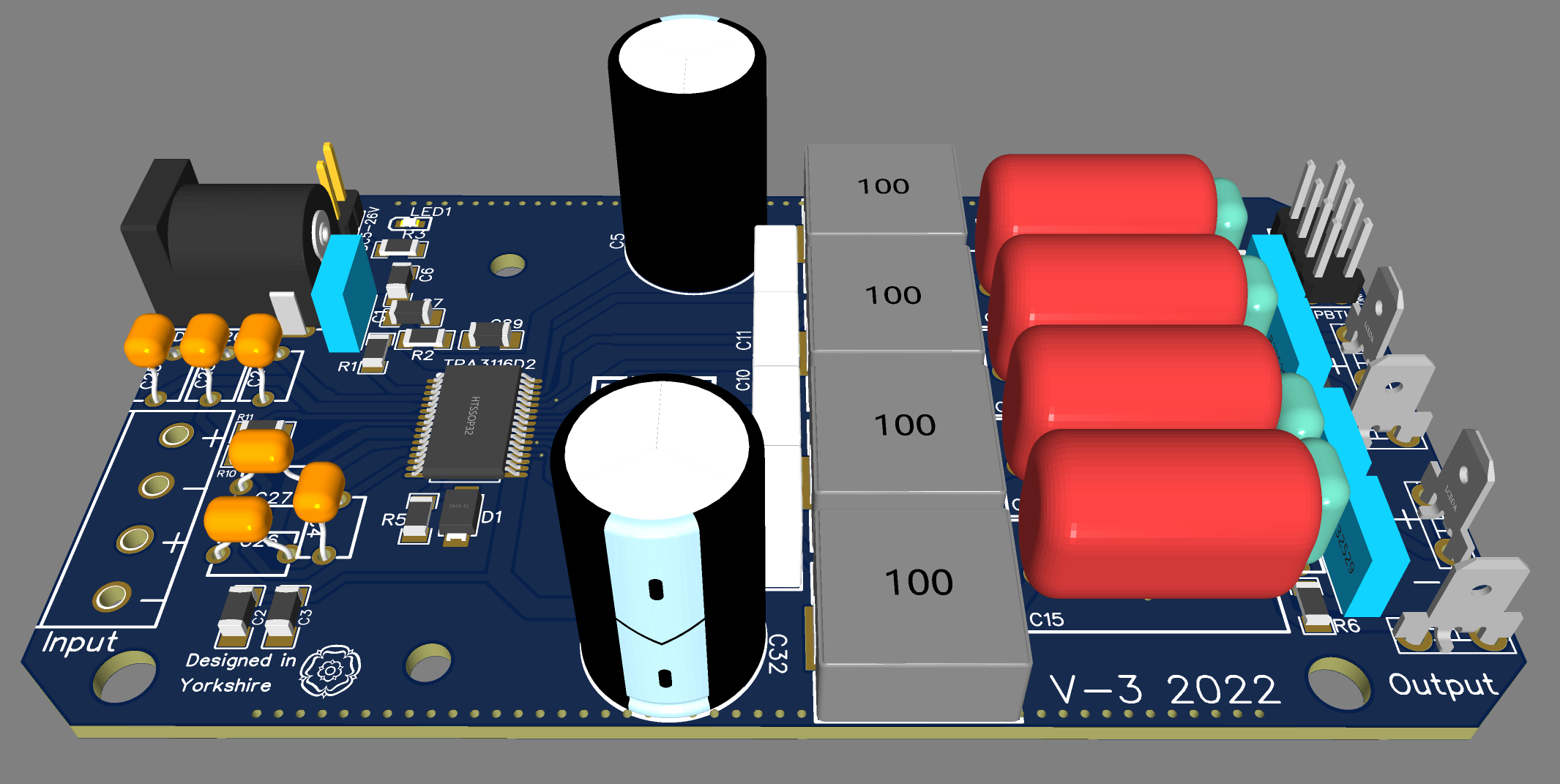
This post is a work in progress
I’ve been building speakers for years, and always had audio electronics as a passion. Up until this point, I have completed many of my own cabinet designs, studying the acoustic sciences to optimise the cabinets.
I’ve used many different types of amplifier with my cabinet designs but have often found the stock solutions might not be perfect fits for the bespoke use case I might want.
As such, I thought the leap to designing my own amp board for a chip amp would be a great step, with the long term vision being to have a fully self designed discrete amplifier board.
Which amp type?
The first decision process in designing a chip amp board, was to evaluate the types of chip amp available and select one based on use case and operational conditions.
“So what’s the difference between A, B, AB, & D?”
I’ll give you a BRIEF explanation, but you can certainly go more in depth on this, so please do your own additional reading if you like.
Let’s start with class A – the key point to note with class A is that the transistors are always on. This means that when the transistors are not amplifying a signal, they are dissipating energy via heat. In addition to these losses, class A amps also amplify the negative voltages equally as they do the positive voltages, further generating heat.
“Okay, so why would I choose a class A, it sounds like they are just inefficient and generate a lot of unnecessary heat?”
That’s right, class A amps do generate a lot of heat and are indeed rather inefficient (~25% efficient). The advantages of such an amplifier, however, can be seen in the distortion free performance. As the transistors aren’t actually switching at all (they are always on) then we don’t have the negative effects of the switching cycles, which include distortion and high frequency switching interference. You won’t often find class A’s around, as they are pretty expensive to buy and run.
Class B amps are the next in the list of architectures. These aren’t too dissimilar from class A, but they use a dual transistor push-pull setup in place of each individual transistor on a class A. One transistor handles the positive side of the wave and the other handles the negative, resulting in around a 50% efficiency increase when compared with the class A. Where this amp class falls behind A, is in the -0.7V to +0.7 range of the signal. In this range, distortion occurs due to the dead band on the input base voltage. True audiophiles would say that these two types of amp are significantly different because of this, however this difference is often negligible to the average listener’s ear.
Class AB amps are the amalgamation of the efficiency of class B and the fidelity of class A. This amp class attempts to mitigate against the dead band voltage range distortion seen in class B’s by allowing each of the two transistors to operate simultaneously. Essentially, each transistor is on for more than half a cycle, but less than a full cycle – this overlap allows for accurate signal reproduction within the voltage range that on class B was distorted.
Class C amps. These amps are very rarely used within the audio space, due to their significant distortion levels. They boast an 80% efficiency as their heavy biasing means output signals sit at 0 for more than half of the sine wave. I won’t cover these deeper as they’re not really relevant.
Class D amplifiers offer a nice balance between power efficiency and sound quality….. **MORE TO BE WRITTEN***
https://www.analog.com/en/technical-articles/fundamentals-of-class-d-amplifiers.html
Based on my previous experience with various class D chip amps, I elected to go with the TPA3116D2 from Texas instruments. I’ve had a few boards that use this chip and have been really impressed with the output and efficiency.
This chip can output two 50W(rms) channels, or a bridged 100W(rms) channel and so is a great power level for my intended use of small to mid size portable speakers.

Circuit Design
“So we’ve selected a chip, now what?”

First job is to download the datasheet from TI and start to review the documentation. There’s a heck of a lot of info in the datasheet, but we’ll just focus on the core info to start.
V_in – We must be sure to check the vin requirements of the chip, the fastest way to find yourself having to reorder new chips is to overvolt it. In this case our rage is 4.5-26v. So let’s keep 26v in mind as our limit. Even better to stay safe and have 25v in mind. (This allows us more leeway in our ripple mitigation later)
For this board design, I’m going to stick with using an external PSU, so the board will be fed with DC. This makes the design a little more simple, but feel free to design an onboard psu if you like. I’ll add an appendix to this post explaining how to design a basic 12v PSU with plenty of power for this chip. Please note that if you go down this road, be sure you are comfortable designing 230v AC power electronics – when these go wrong they often go more wrong than DC. (**Has flashback to many mains shocks and exploding capacitors)
There are a number of pins on the board that we need to set in a particular manner for the configuration we’d like to set. The easiest way to quickly see what we need to do, we can take a glance at the example schematics in the datasheet. Before doing this, I’d recommend you review the pin function table on page 4. Not all these pins might be relevant to how you’d like your chip to operate, but it’s good to still.be familiar with each pin and what it does.

There’s also a table on the next page with the maximum ratings, this is really important to have in your mind as over volting or over heating a component will lead to destruction.

Let’s now head down to page 26 where we’ll find the first typical application circuit diagram. This schematic is fantastic for getting the core design down and basic functions working.

Take some time to review this schematic. It’s a nicely designed chip as you pretty much have inputs on the left and outputs on the right. You should be able to see that we have a dual chip setup, with the first chip running in stereo 50w mode to power L/R tops, and the second chip running in bridge mode to provide 100w to the subs. Note that the chips are tied together via the sync pins, both of which are coupled to ground via a decoupling capacitor.
Looking at the top right and bottom right of each chip, we can see power filtering has been implemented using a polarised capacitor between PVcc and GND. If you know your basic electronic theory, you’ll understand what this is doing. For those who are new to this, it is basically smoothing things out and reducing any ripples and variations in the DC supply voltage to the chip. Along side this cap are a couple of non-polarised caps that are being used as decoupling caps. These address any spikes in the AC component of the voltage.
Setting gain on this chip is nice and simple. You’ll want to review both the table on page 6 and the schematic, so that you know what you need to set the potential divider to to achieve the desired gain.


Breakout boards! Stay away!
I was keen to have a breadboard-able setup that I could use for testing various configurations so I went ahead and ordered the tssop32 breakout board in the image below. Don’t bother trying this, I hadn’t realised but the traces on this breakout board are so thin that they don’t stand a chance in handling the current that the tpa3116 needs. The traces burn out immediately on power up. Do let me know in the comments if anyone knows of an easily accessible tssop32 breakout board that has decent tracks.

PCB Layout
Now that we have our schematic and are happy with the functionality, we need to focus on getting it into a nice PCB layout that doesn’t hinder any of the functions.
I used EasyEDA for this, as it links directly into the JLCPCB ordering system to be able to quickly get prototype board ordered. JLCPCB even offer fully populated boards via their sister company LCSC, which is another reason I went for this. This certainly isn’t the cheapest way to go about this, but it is one of the simplest way of you just want a prototype board making and don’t want to faff about ordering all the components separately – especially if you plan on iterating a few design versions, you don’t want to end up with a spool of 20,000 resistors in a specific package type that you never end using. If you have finalised your design, I’d recommend sticking to just ordering boards and populating them yourself as you’ll save a lot of time and money this way.

Component Selection
Phoenix Contact
When searching for a nice connector that would bring good balance between ease of connection and prototypability, I discovered the company Phoenix contact. They produce a wonderful range of quick connect PCB connectors that are perfect for my use case.

Capacitors
“Polarised, non-polarised, electrolytic, film, ceramic – what in the Helen-of-Troy am I supposed to pick?”
On first approaching this, task it may seem pretty intimidating. Fear not, I’ll try to simplify things for you. Polarised vs non-polarised is an easy one – you can’t mix these up. If your schematic calls for polarised then you MUST use polarised and vice versa.
Now deciding on electrolytic / film / ceramic is a bit of a trickier decision which involves a lot of either reading up on other peoples reported experiences, or doing your own testing. Out of all the components on our board, capacitors are most likely to colour our output.
Resistors
This is a much easier game than the caps – resistors resist, and there isn’t much in terms of selection here aside from manufacturing tolerances and power ratings. Pick ones that can handle the power, and minimize the tolerance so your values don’t vary too much, and you’ll be golden.
Inductors
The main thing to look out for in choosing a coil, is the power rating. These coils are processing the entirety of the output channels, so they will take the brute force of the current peaks. Picking an underrated coil will become pretty quickly apparent as you start to see magic smoke as you crack up the gain.
Heatsink
I hunted around looking for suitable heatsinks for this chip, and stumbled across one that has been specifically designed for the chip, with the capability to dissipate the required heat when operating at full power.
This is the heatsink supplied on the evaluation board from TI. If I go production with this board I will look for another alternative as this one is a bit pricey.
Note: You may just have to throw all of these selections out of the window if LCSC don’t have the ones you need, so get ready for that rollercoaster when you go to order


In parallel to my design work on this board, my friend worked on a DSP board based around the ADAU1701, read their blog post about it here. These boards work in harmony to create a really nice portable or home audio setup.
